Key Specifications
Package: SOP
Mount Type: Surface Mount
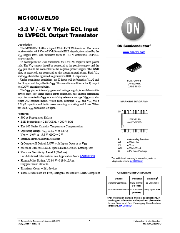
Pins: 20
Operating Voltage: 3.3 V
Max Voltage (typical range): 3.8 V
Min Voltage (typical range): 3 V
Logic Function: Translator
Length: 12.8 mm
Width: 7.5 mm
Max Operating Temp: 85 °C
Min Operating Temp: -40 °C
| Part | MC100LVEL90 |
|---|---|
| Description | Triple ECL to PECL Translator |
| Manufacturer | onsemi |
| Size | 132.77 KB |
Triple ECL to PECL Translator
The MC100LVEL90 is a triple ECL to LVPECL translator. The device receives either -3.3 V or -5 V differential ECL signals, determined by the VEE supply level, and translates them to +3.3 V differential LVPECL output signals.
500 ps Propagation Delays
ESD Protection: > 2 kV HBM, > 200 V MM
The 100 Series Contains Temperature Compensation
Operating Range: VCC = 3.0 V to 3.8 V; VEE = -3.0V to -5.5 V; GND = 0 V
Internal Input Pulldown Resistors
Pricing from 8.56971 USD, available from Avnet and Verical.
Powered by Octopart
Price & Availability
| Seller | Price Breaks | Buy |
|---|---|---|
| Avnet | 1000+ : 8.56971 USD 2000+ : 8.10649 USD 4000+ : 7.89316 USD 8000+ : 7.69077 USD |
View Offer |
| Verical | 38+ : 9.875 USD 100+ : 9.3875 USD 500+ : 8.8875 USD 1000+ : 8.4 USD |
View Offer |